


By Jack Chang/Fortune Times
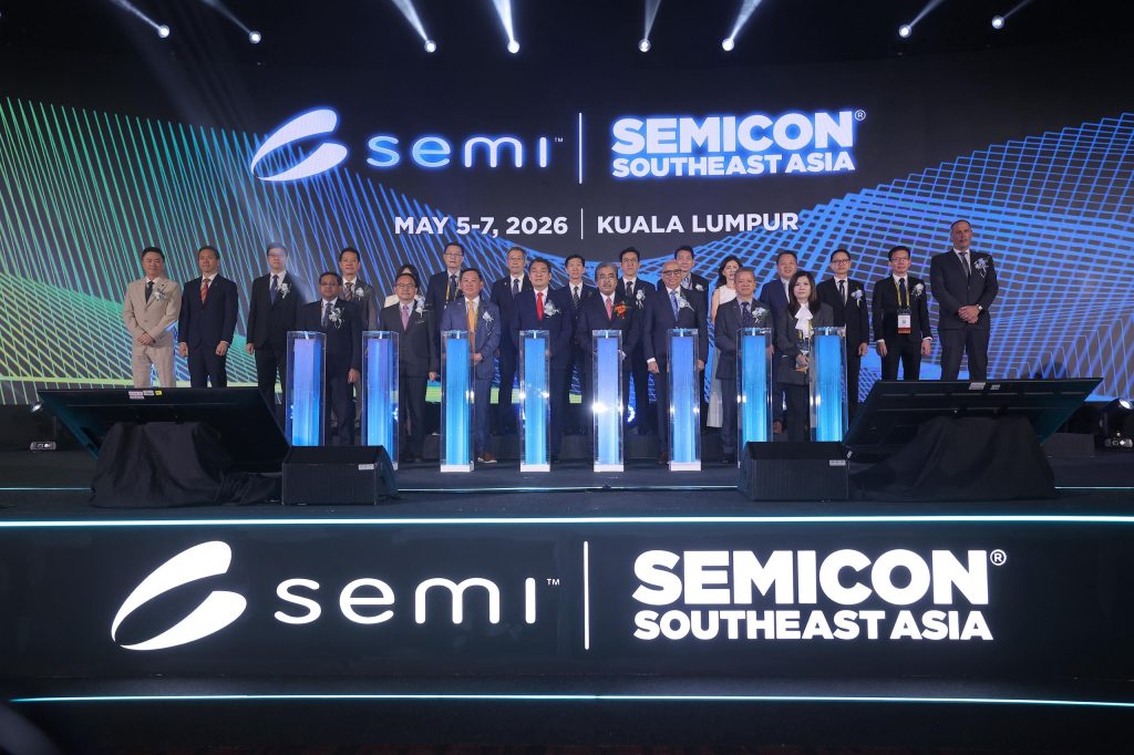
(Kuala Lumpur, 06.05.2026) In an era where artificial intelligence is driving an explosion in computing demand, competition in the semiconductor industry is no longer just about “who can make chips smaller,” but about “who can build complex systems at lower cost, in shorter cycles, and with higher efficiency.”
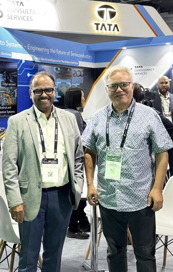
During 2026 SEMICON Southeast Asia held in Kuala Lumpur, Tata Consultancy Services (TCS) Vice President and Chief Technology Officer Prasad Patchigolla, in an interview with Fortune Times, pointed out that the global semiconductor industry is entering a phase of structural restructuring. Chiplet architectures, AI-driven manufacturing, and the rebalancing of regional supply chains will become the three key variables shaping the industry landscape in the coming years.
Chiplets refer to breaking down a highly integrated single chip into multiple smaller functional chip modules, which are then recombined into a complete system through advanced packaging. This approach allows companies to avoid concentrating all functions into a single large chip and also eliminates the need for every module to use the most advanced and expensive process node, thereby achieving a new balance among performance, cost, yield, and development cycle.
Prasad believes that the rise of chiplets is not merely a technological upgrade, but an inevitable choice for the semiconductor industry to address complexity and cost pressures.
He noted that chip complexity is currently growing exponentially, while design and manufacturing costs continue to rise, and product cycles are becoming longer. Traditional chip development models are no longer able to bear such pressures alone. The value of chiplet architecture lies in providing a more flexible, modular, and cost-efficient solution.
In response to this trend, TCS is increasing its investments in two areas: on the engineering side, including advanced packaging design and interconnect standards such as UCIe; and on the manufacturing side, promoting fab process automation through artificial intelligence to improve efficiency and process stability.
Prasad believes that the core competitiveness of semiconductor companies in the future will not only lie in single-point technological breakthroughs, but in system-level integration capabilities across design, packaging, manufacturing, and software engineering.
However, Prasad does not believe that AI will immediately replace human labor. Especially in a high-complexity and high-risk industry like semiconductor manufacturing, many critical decisions still require engineering judgment. The more realistic role of AI today is that of an “intelligent co-pilot,” helping engineers identify problems faster, make more accurate judgments, and manage processes more effectively.
This means that the future of semiconductor manufacturing will not be a fully “lights-out factory” overnight, but rather a highly efficient system based on human–machine collaboration.
Beyond technological pathways, the geographic landscape of the global semiconductor industry is also evolving. India is gradually moving from its traditional role focused on chip design and engineering services toward becoming a manufacturing participant. With the introduction of fabs and OSAT capabilities, India’s semiconductor ecosystem is evolving from a single design capability toward a more complete industrial chain. Domestic companies, including those within the Tata Group, are increasing investments on both the design and manufacturing fronts.
At SEMICON Southeast Asia 2026, companies from China, Malaysia, and Singapore were highly active, with emerging technologies such as 3D-printed advanced packaging demonstrating a clear rise in innovation capability.
At the same time, Southeast Asia is becoming increasingly important in the restructuring of the global semiconductor supply chain. Prasad believes that over the next five years, the region will become a key growth area for fabs, advanced packaging, semiconductor equipment manufacturing, and local innovative companies. It is not only a destination for capacity relocation, but also a place where technological innovation is emerging.
“In the past, most industry innovation came from Europe and the United States. This time, I see more and more leading innovation emerging locally in Southeast Asia,” Prasad said. He also emphasized that chips have become the core infrastructure of the AI era. Whether it is model training, inference applications, or data storage, all rely on semiconductor support. Although the storage industry will continue to experience cyclical fluctuations, the long-term trend of data growth will not reverse, and demand for storage will continue to expand.
From chiplets to AI-driven manufacturing, from India’s rise to Southeast Asia’s opportunities, Prasad identifies a clear trend: the global semiconductor industry is shifting from a single-dimensional technology race to a comprehensive competition based on system capabilities, regional positioning, and intelligent manufacturing.
As the semiconductor industry moves toward greater complexity and scale, the emphasis is shifting to organizations like TCS that can operate at scale across silicon and embedded engineering to fabrication. What is increasingly valuable is the ability to combine deep chip‑level expertise with system‑level and manufacturing intelligence, turning breakthrough concepts into production‑ready realities. In this emerging model, AI plays a central role—not just as a workload driver, but as the connective tissue of the fab, embedding intelligence into process control, yield engineering, and operational decision‑making. The semiconductor leaders of the next decade will be those who can industrialize innovation at speed, translating bold engineering ideas into safe, scalable systems that power an AI‑native world.